At the beginning of April 2019, the second stage of R & D on the topic “Development of large-format high-resolution X-ray detectors with high radiation resistance, and the development of their production technology” was successfully completed under the STC-MT agreement with the Federal State Budgetary Institution "Fund for the Promotion of small enterprises development in the Scientific and Technical Field".
In the course of the work on the second stage of R & D, the following results were obtained:
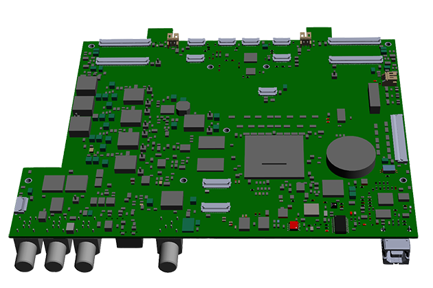
- The development of circuit solutions for detector electronic environment has been carried out. The circuit diagrams of the electronic modules of the detector environment have been developed. Based on them, gerber files were prepared for the manufacture of printed circuit boards of the detector environment modules.
- The design of the detector has been developed. A set of working design documentation for the detector has been prepared.
- The technology of combining photosensors has been developed. Working design documentation for a photosensor combining stand has been developed.
- The technology for installing scintillators on photosensors has been developed. Design documentation has been developed for a fiber optic scintillator installation stand.
- The development of a system for monitoring the temperature regimes of the detector has been carried out. A circuit design is proposed for an integrated temperature sensor located in the ADC PS zone.
- Work was carried out to ensure the radiation resistance of the detector. The design of the detector provides for the use of a fiber-optic plate with a combined scintillator based on CsI: Tl and Gd2O2S: Tb. The structures of CMOS transistors of the photosensor: p-channel - with induced channel, n-channel - with built-in channel. The use of Si3N4 is provided as a dielectric of photosensor elements.
The tasks of the second stage of R & D were solved in full, in accordance with the schedule and allowed to proceed to the implementation of the works of the third stage.
