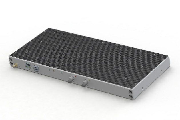
At the beginning of October 2018, the first stage of R&D on the topic “Development of large-format high-resolution X-ray detectors with high radiation resistance, and the development of their production technology” was successfully completed under the STC-MT agreement with the Federal State Budgetary Institution "Fund for the Promotion of small enterprises development in the Scientific and Technical Field".
In the course of the work on the first stage of R&D using modern methods of digital modeling of optical and electrical processes, the circuit and topological architecture of the pixel were developed. For the proposed pixel schematic diagram, optimal levels of supply and bias voltages were calculated. Based on the obtained concept, the topology of the photocell was worked out using the 180 nm process libraries. An innovative element of the solution is the approach that allowed combining the pixels into groups that form the hybrid larger photocell. The optimal pixel size is determined. A draft design of the photo sensor is developed.
The optimal structure of the high-energy X-ray conversion stack is determined and a draft design of a flat panel detector is developed using digital modeling of optical stacks of various compositions.
The tasks of the first stage of R&D are solved in full, in accordance with the schedule and allowed to proceed to the implementation of the works of the second stage.
